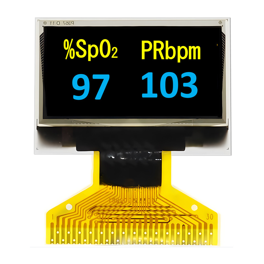
0.96 Inch Thin OLED Display Dual Color Yellow+Blue SPI Interface
Product Introduction
Product Quick Review
►Model No. SFOS096JY-7149AN
►Thin OLED Display
►0.96" OLED Display, OLED 0.96"
►Suitable for wearable device
►Type: Graphic
►Structure: COG
►128 x 64 Dot Matrix
►IC:SSD1315
►3V Power supply
►1/64 duty
►Interface: 6800, 8080, SPI, I2C
►Display Color: Dual Color Yellow+Blue
Description
SAEF released a LOW COST 0.96 inch Thin OLED Display
SFOS096JY-7149AN model which is made of 128x64 pixels, diagonal
size only 0.96 inch. The new version thin 0.96" OLED display is
also built-in SSD1315 driver IC; it communicates via 6800/8080
8-bit parallel and I2C/SPI interface. Adopting thinner OLED panel
is a new trend, for new projects, we recommend customers to choose
the thinner SFOS096JY-7149AN for new design
projects.SFOS096JY-7149AN module supports internal Charge Pump
supply and external VCC supply.
Product Information
| Product: | 0.96" Inch Graphic OLED |
| Resolution: | 128x64 |
| Color: | Yellow+Blue (Dual Color) |
| Module Size: | 24.74*16.9*1.42 (mm) |
| Controller: | SSD1315 |
| Pin Number: | 30 Pins |
| Life Time: | 50,000 Hours |
| Contrast Ratio: | 20,000 : 1 |
| Optics: | All Viewing Angles |
| Glass: | OLED |
| Operating Temp: | -40°C To +80°C |
| Interfaces: | 6800/8080 Parallel, 4-wire SPI, And I2C |
| Brightness: | 180 Nits |
| Compliance: | REACH & RoHS Compliant |
0.96 Inch Thin OLED Display Dual Color Yellow+Blue SPI Interface
Product Drawing

Pin Definition
| No. | Symbol | Function |
|---|
| 1 | N.C. (GND) | Reserved Pin (Supporting Pin)
The supporting pins can reduce the influences from stresses on the
function pins. These pins must be connected to external ground. |
| 2 | C2P | Positive Terminal of the Flying Inverting Capacitor Negative
Terminal of the Flying Boost Capacitor The charge-pump capacitors
are required between the terminals. They must be floated when the
converter is not used. |
| 3 | C2N |
| 4 | C1P |
| 5 | C1N |
| 6 | VBAT | Power Supply for DC/DC Converter Circuit
This is the power supply pin for the internal buffer of the DC/DC
voltage converter. It must be connected to external source when the
converter is used. It should be connected to VDD when the converter
is not used. |
| 7 | NC | NC |
| 8 | VSS | Ground of Logic Circuit
This is a ground pin. It acts as a reference for the logic pins. It
must be connected to external ground. |
| 9 | VDD | Power Supply for Logic
This is a voltage supply pin. It must be connected to external
source. |
| 10 | BS0 | Communicating Protocol Select
These pins are MCU interface selection input. See the
following table:
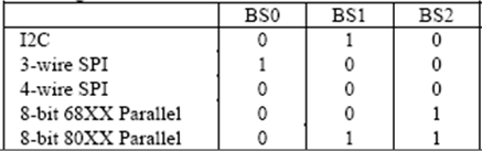 |
| 11 | BS1 |
| 12 | BS2 |
| 13 | CS# | Chip Select
This pin is the chip select input. The chip is enabled for MCU
communication only when CS# is pulled low. |
| 14 | RES# | Power Reset for Controller and Driver
This pin is reset signal input. When the pin is low, initialization
of the chip is executed. |
| 15 | D/C# | Data/Command Control
This pin is Data/Command control pin. When the pin is pulled high,
the input at D7~D0 is treated as display data.
When the pin is pulled low, the input at D7~D0 will be transferred
to the command register. For detail relationship to MCU interface
signals, please refer to the Timing Characteristics Diagrams.
When the pin is pulled high and serial interface mode is selected,
the data at SDIN is treated as data. When it is pulled low, the
data at SDIN will be transferred to the command register. In I2C
mode, this pin acts as SA0 for slave address selection. |
| 16 | R/W# | Read/Write Select or Write
This pin is MCU interface input. When interfacing to a 68XX-series
microprocessor, this pin will be used as Read/Write (R/W#)
selection input. Pull this pin to “High” for read mode and pull it
to “Low” for write mode.
When 80XX interface mode is selected, this pin will be the Write
(WR#) input. Data write operation is initiated when this pin is
pulled low and the CS# is pulled low. |
| 17 | E/RD# | Read/Write Enable or Read
This pin is MCU interface input. When interfacing to a 68XX-series
microprocessor, this pin will be used as the Enable (E) signal.
Read/write operation is initiated when this pin is pulled high and
the CS# is pulled low.
When connecting to an 80XX-microprocessor, this pin receives the
Read (RD#) signal. Data read operation is initiated when this pin
is pulled low and CS# is pulled low. |
| 18~25 | D0~D7 | Host Data Input/Output Bus
These pins are 8-bit bi-directional data bus to be connected to the
microprocessor’s data bus. When serial mode is selected, D1 will be
the serial data input SDIN and D0 will be the serial clock input
SCLK. When I2C mode is selected, D2 & D1 should be tired together
and serve as SDAout & SDAin in application and D0 is the serial
clock input SCL. |
| 26 | IREF | Current Reference for Brightness Adjustment
This pin is segment current reference pin. A resistor should be
connected between this pin and VSS. Set the current lower than
12.5μA. |
| 27 | VCOMH | Voltage Output High Level for COM Signal
This pin is the input pin for the voltage output high level for COM
signals. A capacitor should be connected between this pin and VSS. |
| 28 | VCC | Power Supply for OEL Panel
This is the most positive voltage supply pin of the chip. A
stabilization capacitor should be connected between this pin and
VSS when the converter is used. It must be connected to external
source when the converter is not used. |
| 29 | VLSS | Ground of Analog Circuit
This is an analog ground pin. It should be connected to VSS
externally. |
| 30 | NC
(GND) | Reserved Pin (Supporting Pin)
The supporting pins can reduce the influences from stresses on the
function pins. These pins must be connected to external ground. |
0.96 Inch Thin OLED Display Dual Color Yellow+Blue SPI Interface
Product Image

Factory Facilities and Certificates


Contact Us
We love to hear about your projects, If you have any questions, we
can be reached at sales2@saef.com.cn
Search Keyword: 0.96 oled, oled 0.96, 0.96 inch oled, oled 0.96
inch, 0.96 i2c oled, 0,96 inch i2c oled, 0.96 inch white oled, 0.96
inch blue oled,


